Language

8-inch SiC Wafers

Deep Expertise in Core SiC Process Technologies
Significantly Enhances Overall Wafer Competitiveness

Innoevsic has strategically deployed a fully automated 8-inch SiC wafer production line. Leveraging proprietary planar and trench device architectures, industry-leading process equipment and technologies, and a comprehensive inspection system, we significantly enhance production efficiency and yield, delivering highly competitive domestically developed SiC wafers.

Key Technologies

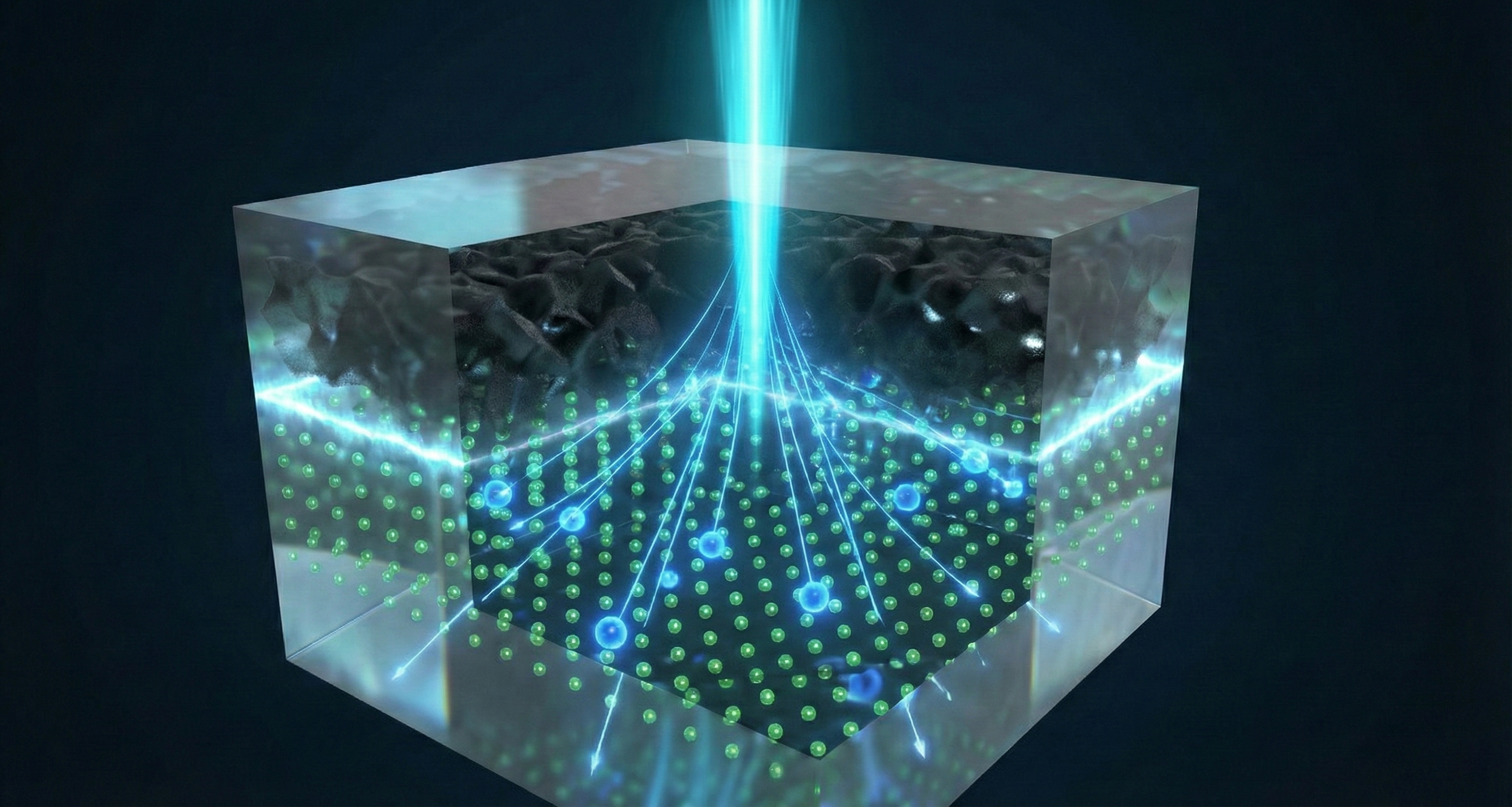
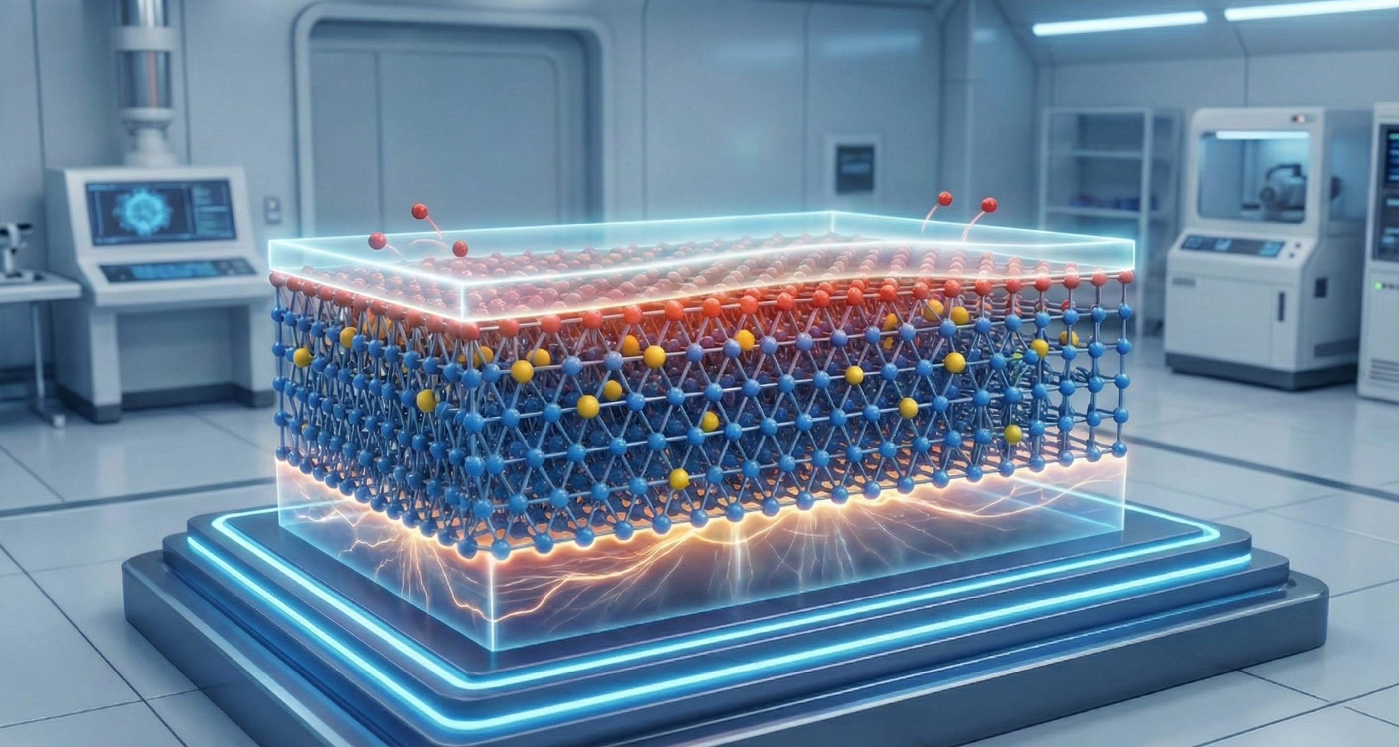
Deep Ion Implantation Technology

Advanced high-energy, high-current, and high-temperature deep ion implantation technology enables precise control of doping depth and concentration profiles, forming optimized doping structures in target regions. Through lattice damage suppression and activation mechanisms, the technology significantly reduces device on-resistance, ensuring device performance and consistency.

逻辑节点相关图片

High-Temperature Activation and Surface Repair Technology

High-temperature activation and surface damage repair processes ensure dopants fully migrate and occupy lattice sites, significantly enhancing device electrical activity and voltage withstand capability. The surface damage repair process effectively prevents roughness increase caused by silicon evaporation, maintains interface flatness, improves breakdown voltage and long-term reliability, providing a solid foundation for stable operation of high-voltage devices.

像素技术相关图片

Precision Etching and Edge-Smoothing Technology

Through optimized etching and subsequent thermal treatments, the corner-rounding precision of device edges and the control of sidewall roughness are achieved. This effectively mitigates electric-field concentration, significantly enhances oxide growth quality, and improves interface reliability. The process ensures stable breakdown behavior under high-voltage conditions, establishing a critical technological foundation for the design of highly reliable SiC devices.

功率器件工艺相关图片

High-Quality Gate Oxide Technology

Through optimized pre-treatment, low-temperature uniform growth, and subsequent thermal processing, a high-quality gate oxide layer with extremely low defect density and high electron mobility is formed. This effectively reduces leakage current and threshold voltage drift, enabling long-term stable operation of devices under high-temperature and high-voltage conditions, ensuring product performance consistency and reliability.

先进封装与测试相关图片

Low-Resistance Silicide Technology

During the silicide formation process at the source and drain regions, precise control of metal selection, film thickness, and thermal/laser annealing Parameters enables extremely low sheet resistance and contact resistance. This technology not only significantly reduces device on-resistance but also provides excellent thermal stability and anti-aging characteristics, offering dual guarantees of high efficiency and high reliability for Innoevsic's SiC power devices.

功率器件工艺相关图片)